Table of Contents
DIODE
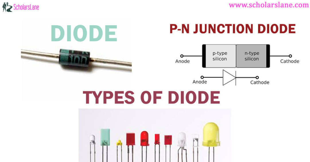
A diode is a two-terminal electronic component (with anode and cathode) that only conducts current in one direction (as long as it is operated within a specified voltage range).
An ideal diode always shows zero resistance in the forward direction and infinite resistance in the reverse direction.
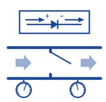
Semiconductor diode schematic symbol: Arrows in the symbol indicate the direction of current flow
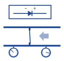
Hydraulic Check Valve Analogy
- Flow permitted
- Flow prohibited
- Check valves are the device used to control the flow of pressure or any fluid: they open and allow flow if the pressure across them is in the right direction to open the gate (in this analogy shown, greater fluid pressure on the right than on the left). If the pressure is in the backward direction the pressure difference across the check valve will close and hold the gate so that no flow occurs.
- Like check valves, diodes are pressure operated (voltage-operated) devices. The main difference between forward-bias and reverse-bias is the polarity of the voltage across the diode.
History of Diode
In the year 1940 at Bell Labs, Russell Ohl was working with a silicon crystal to find out its properties. One day accidentally when the silicon crystal which has a crack in it was exposed to the sunlight, he found the flow of current through the crystal and that was later called a diode, which was the beginning of the semiconductor era.
Construction of Diode
Diode is made up by joining P and N-type semiconductors together result in the formation of the P-N junction diode.
The diode word can be explained as ‘Di’ meaning two and ‘ode’ is taken from the electrode. This component has two terminals or electrodes (one connected to P-side and the other to the N-side).The terminal connected to P-side material is called Anode and the terminal connected to N-side material is called Cathode.
Types of diode
- ZENER DIODE
- SMALL SIGNAL DIODE
- LARGE SIGNAL DIODE
- LIGHT EMITTING DIODE (LED)
- CRYSTAL DIODE
- CONSTANT CURRENT DIODE
- SCHOTTKY DIODE
- SHOCKLEY DIODE
- PIN DIODE
- AVALANCHE DIODE
- GUNN DIODE
- STEP RECOVERY DIODE
- TUNNEL DIODE
- VARACTOR DIODE
- LASER DIODE
- TRANSIENT VOLTAGE SUPPRESSION DIODE
- GOLD DOPED DIODE
- SUPER BARRIER DIODE
- PELTIER DIODE
- SILICON CONTROLLED RECTIFIER
- VACCUME DIODE
P-N Junction Theory
A diode is made with P and N-type semiconductors but we need to know what exactly happens inside it to form a unique property of allowing current in only one direction, not in other direction and what happens at its junction.
Junction Formation
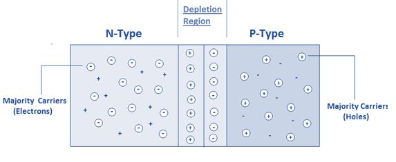
Initially, when both the materials are joined together (without any external voltage applied) the excess electrons in the N-type and excess holes in the P-type will get attracted to each other and gets recombined where the formation of immobile ions (Donor ion and Acceptor ion) takes place as shown in below picture. These immobile ions resist the flow of electrons or holes through it which now acts as a barrier in between the two materials (formation of the barrier means the immobile ions diffuses into P and N regions). The barrier formed is known as Depletion region and width of the depletion region, depends upon the doping concentration in the materials.
If the doping concentration is equal in both the materials then the immobile ions diffuse into both the P and N materials equally.
If the doping concentration differs the width of the depletion region also differs. Its diffusion is more into the lightly doped region and less into the heavily doped region.
P-N junction diode when unbiased.
Working configuration of the diode
Diode works in 2 different working configurations depending upon the applied voltage across the terminal.
Forward Bias Diode Configuration
If a positive end of the battery or a voltage source is applied to the anode of the diode and negative end to the cathode of the diode then it is in the forward-biased.
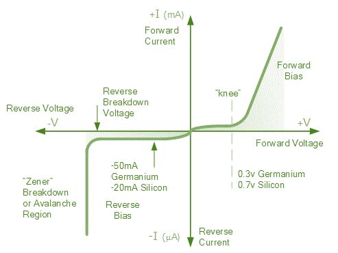
To make the diode conduct first we need to break the barrier formed in the path. External voltage should be applied to the terminal of the diode to break the nominal voltage of +0.7 Volts (for Silicon) and +0.3 Volts (for Germanium. These voltages are called as Cut-in voltage or Break-point voltage or Offset voltage or Threshold voltage. Current will not flow until these voltages are very less.
Due to forward bias, majority charge carriers in both regions get repelled (because the positive voltage is applied to the P region and negative to N region) and enter into the depletion region. Hence immobile ions get back lost carriers become neutral and move to un-depleted region hence the width of the barrier decreases gradually when the applied voltage is greater than or equal to cut-in voltage, the entire barrier is destructed and the electrons and holes are now free to cross the junction which then forms a closed circuit and enables the flow of current.
A diode in forward bias acts as a closed switch and has a forward resistance of few ohms (around 20Ω).
Diode Equation
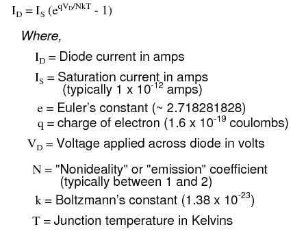
forward voltage drop is more complex. An equation is used to describes the current of the diode, with the given constant voltage dropped across the junction, the temperature of the junction, and several physical parameters. It is commonly known as the diode equation:
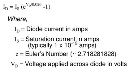
The term kT/q is the voltage produced within the P-N junction due to the action of temperature and is known as the thermal voltage or Vt of the junction. At room temperature, this is around 26 millivolts. Knowing this, and assuming a nonideal coefficient of 1, we can simplify the diode equation as
Reverse bias Diode Configuration
If the negative terminal of a voltage source is applied to the anode or P region of the diode and positive terminal to the cathode or N region of the diode, it is said to be reverse biased.
When such voltage is applied, the majority charge carriers in both regions get attracted to source such that large numbers of immobile ions are created and enter into the P and N regions. Therefore, the width of the depletion region also increases gradually which is now difficult for the electrons and holes to cross the junction so open circuit forms and current flows. But if we continue increasing the voltage, at a point barrier or depletion region cannot withhold the external force and the junction breaks down which may sometimes cause the normal diode damaged forever or permanently. To control this we can heavily dope the regions and put the diode safe, this feature can be seen in Zener diodes.
The voltage at which the diode conducts in reverse bias is known as break down voltage.
The diode in reverse bias acts as an open switch, it has a resistance of Megaohms
On applying, the reverse voltage to the diode small amount of current flows through the circuit due to the minority charge carriers which is known as Reverse saturation current or leakage currents because even when the diode is open-circuited, current remains in the circuit so it is termed as leakage.
The maximum reverse-bias voltage rating of a diode is known as the Peak Inverse Voltage, or PIV, and can be obtained from the manufacturer datasheet. PIV rating of a diode also varies with temperature, but that PIV increases with increased temperature and decreases with a decrease in temperature exactly opposite that of forward voltage.
V-I Characteristic of a Diode
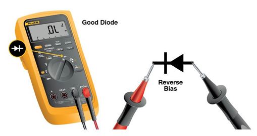
How to check a diode with Multimeter
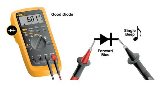
A digital multimeter can be used to test the diode working condition by selecting the diode option in the multimeter dial. The multimeter produces enough voltage so it can cross its barrier potential.
The forward-biased resistance of a working diode is in the range from 10 to 1000 ohms.
While measuring in reverse bias, a digital multimeter will show the OL reading which means very high resistance.
Diode ratings
There are many other parameters of diodes important for the circuit design and component selectionin addition to the forward voltage drop (Vf) and peak inverse voltage (PIV),.Detailed specifications of the products( including diodes) are always provided by Semiconductor manufacturers in the publications known as datasheets
A diode datasheet will contain the following parameters:
Maximum repetitive reverse voltage(VRRM):-Highest voltage a diode can withstand in reverse bias condition. Ideally, it is infinite.
Maximum DC reverse voltage (VR or VDC):- It is the highest voltage a diode can withstand in reverse-bias configurationcontinually. Ideally, it is infinite.
Maximum forward voltage(VF):-Ideally this is zero but practically this is described by diode equation and specified by the manufacturer in a datasheet
Maximum (average) forward current(IF(AV)):- the highest average amount of current diode can conduct in forward bias mode. Ideally, this value should be infinite but in practicality, it is limited by junction thermal capacity.
Maximum (peak or surge) forward current(IFSM):- the highestpeak a current diode can conduct in forward bias mode.In the ideal case, this value is infinite but in practicality, it is limited by junction thermal capacity.
Maximum total dissipation(PD):- Total amount of power allowed for a diode to dissipate during operation in forward bias, higher the power dissipation higher the working temperature of the diode.
Operating junction temperature(TJ):- the highest tolerable temperature for the diode’s PN junction, usually given in degrees Celsius (oC) if junction temperature reaches more than the highest limit of diode then thermal break down happens.
Storage temperature range(TSTG):-The range of temperature in which the diode can be stored if the storage temperature range exceeds the value it may damage the component.
Maximum reverse current(IR):- It is the highest amount of reverse current that is allowed when diode is working in forward bias
Typical junction capacitance(CJ):-thevalue of capacitance between the junction, due to the depletion region acting as a dielectric separation between the positive and negative terminal of diode. It is in the range of picofarads (pF).
Reverse recovery time(trr):- It is the total time taken by the diode to turn off itself when changing its polarity from forward bias to reverse bias.

